

Pinout
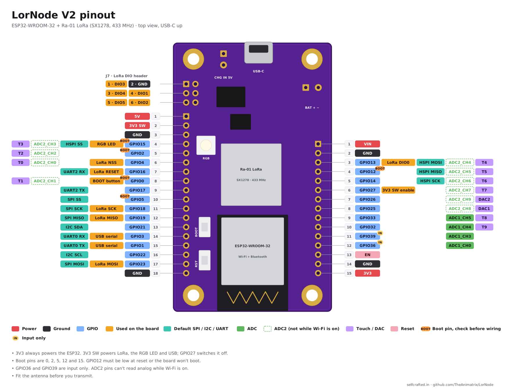
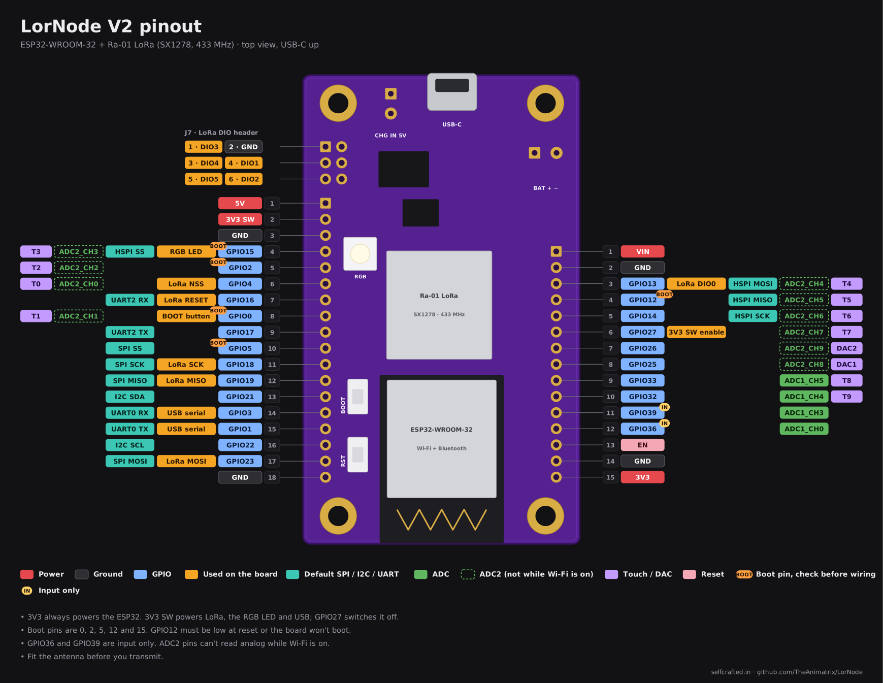
There is also a dark version of the diagram. Both are drawn straight from the KiCad board files, so they match the board.
How to read the diagram
The board is shown from the top, with the USB-C connector pointing up.
- J3 is the left header, 18 pins. Pin 1 is at the USB end.
- J2 is the right header, 15 pins. Pin 1 is at the USB end.
- J7 is the small 2 x 3 header near the top left. It carries the LoRa module's spare DIO pins.
Each pin has a row of coloured chips next to it. Reading outward from the board, you get the pin number and its name first. The chips after that show what else the pin can do: what the board already uses it for, its default bus job (SPI, I2C, UART), its ADC channel, and touch or DAC. The legend under the diagram explains the colours.
The labels printed on the board are shorter than the names in the diagram:
| Printed on the board | Means |
|---|---|
A plain number, like 21 |
That GPIO, so GPIO21 |
SCK, MI, MO |
GPIO18, GPIO19, GPIO23 (the SPI bus) |
RX, TX |
GPIO3, GPIO1 (USB serial) |
EN2 |
GPIO27, which switches the 3V3 SW rail |
I36, I39 |
GPIO36, GPIO39 (input only) |
EN |
The ESP32's reset pin |
L1 to L5 |
DIO1 to DIO5 of the LoRa module |
Which pins should I use?
If you just want to connect a sensor or a button, start with these. Nothing on the board uses them and they have no surprises.
| Pins | Good for |
|---|---|
| GPIO21, GPIO22 | I2C (SDA, SCL). These are the Arduino defaults. |
| GPIO17 | Anything digital |
| GPIO32, GPIO33 | Anything digital, and analog input that keeps working with Wi-Fi on |
| GPIO25, GPIO26 | Anything digital, and DAC output |
| GPIO14 | Anything digital |
| GPIO36, GPIO39 | Inputs only, including analog input that keeps working with Wi-Fi on |
GPIO2, GPIO5 and GPIO12 are free too, but they are boot pins. Read the next section before you use them.
Cautions
Boot pins: 0, 2, 5, 12, 15
The ESP32 reads these five pins at the moment it resets to decide how to start. Whatever you connect to them must not hold them at the wrong level during reset. After the board has started, they work like normal pins.
- GPIO12 must be low at reset, or the board will not boot. This is the one that catches people. Don't connect anything to GPIO12 that pulls it high at power-up, such as a sensor with a pull-up resistor.
- GPIO0 is the BOOT button. Low at reset puts the ESP32 into upload mode.
- GPIO2 must be low or floating at reset for uploads to work.
- GPIO5 should not be pulled up or down at reset.
- GPIO15 is used by the RGB LED. If it is low at reset the ESP32 prints no boot log.
Input only: 36, 39
GPIO36 and GPIO39 can read but not drive. They also have no internal pull-up or pull-down, so a button on these pins needs its own resistor.
ADC2 pins don't read with Wi-Fi on
The ESP32 has two analog converters. Wi-Fi takes over the second one (ADC2), so analogRead() fails on ADC2 pins while Wi-Fi is on. That affects GPIO0, 2, 4, 12, 13, 14, 15, 25, 26 and 27 on the headers. They still work fine as digital pins.
If your sketch uses Wi-Fi and needs analog input, use GPIO32, 33, 36 or 39. Those are on ADC1 and are not affected.
Pins the board already uses
These pins are on the headers, but something on the board is connected to them too.
| GPIO | Used for | Can I still use it? |
|---|---|---|
| 4 | LoRa chip select (NSS) | Leave it alone if you use LoRa |
| 16 | LoRa reset | Leave it alone if you use LoRa |
| 13 | LoRa DIO0 (packet interrupt) | Leave it alone if you use LoRa |
| 18, 19, 23 | SPI bus to the LoRa module (SCK, MISO, MOSI) | Yes, for other SPI devices. Give each one its own chip-select pin. |
| 15 | RGB LED data | Leave it alone if you use the LED |
| 27 | Switches the 3V3 SW rail | No. Use LorNode.peripheralPower() instead. |
| 0 | BOOT button | Best left alone |
| 1, 3 | USB serial (TX, RX) | Not if you want Serial over USB |
Two more pins are used on the board and are not on a header: GPIO35 reads the battery voltage and GPIO34 senses the 5 V input.
One trap: Arduino's Serial2 uses GPIO16 for RX by default, and GPIO16 is the LoRa reset line. If you need a second serial port, give it other pins:
Serial2.begin(9600, SERIAL_8N1, 25, 26); // RX on GPIO25, TX on GPIO26The library has a named constant for every pin, such as LORNODE_LORA_NSS and LORNODE_GPIO21. See the Library reference.
The LoRa DIO header (J7)
J7 brings out DIO1 to DIO5 of the Ra-01 module, printed L1 to L5, plus a ground pin. They are not connected to the ESP32. The LoRa library only needs DIO0, which is already wired to GPIO13. If your own code needs another DIO line, run a jumper wire from J7 to a free GPIO.
Power pins
| Pin | What it is |
|---|---|
| 3V3 | Always-on 3.3 V from regulator 1. This is the rail that powers the ESP32. |
| 3V3 SW | Switched 3.3 V from regulator 2. It powers the LoRa module, the RGB LED and the USB chip. |
| 5V | 5 V from USB-C or the CHG IN pads. Only there while one of them is plugged in. |
| VIN | The input of the 3.3 V regulators. That is the battery voltage, or the 5 V input minus a diode drop while 5 V is plugged in. |
| GND | Ground |
| EN | Pull low to reset the ESP32. Same as pressing RST. |
3V3 or 3V3 SW?
Both give you 3.3 V. The difference is when.
- 3V3 SW is on by default, and goes off when your sketch calls
LorNode.peripheralPower(false)orLorNode.sleepFor(). Power a sensor from here if you want it to switch off while the board sleeps. This is what the sensor examples do. - 3V3 stays on as long as the board has power, including during deep sleep. Power something from here only if it has to stay on while the board sleeps, and remember it will keep drawing current the whole time.
VIN is not regulated. It follows the battery, so don't feed a 3.3 V part from it.
More on the rails in Power and battery.
Full pin table
J3 · Left header
| Pin | Printed | Name | Used on the board | Default function | ADC | Touch / DAC | Watch out |
|---|---|---|---|---|---|---|---|
| 1 | 5V | 5V | – | – | – | – | – |
| 2 | – | 3V3 SW | – | – | – | – | – |
| 3 | GND | GND | – | – | – | – | – |
| 4 | 15 | GPIO15 | RGB LED | HSPI SS | ADC2_CH3 | T3 | boot pin, no ADC with Wi-Fi |
| 5 | 2 | GPIO2 | – | – | ADC2_CH2 | T2 | boot pin, no ADC with Wi-Fi |
| 6 | 4 | GPIO4 | LoRa NSS | – | ADC2_CH0 | T0 | no ADC with Wi-Fi |
| 7 | 16 | GPIO16 | LoRa RESET | UART2 RX | – | – | – |
| 8 | 0 | GPIO0 | BOOT button | – | ADC2_CH1 | T1 | boot pin, no ADC with Wi-Fi |
| 9 | 17 | GPIO17 | – | UART2 TX | – | – | – |
| 10 | 5 | GPIO5 | – | SPI SS | – | – | boot pin |
| 11 | SCK | GPIO18 | LoRa SCK | SPI SCK | – | – | – |
| 12 | MI | GPIO19 | LoRa MISO | SPI MISO | – | – | – |
| 13 | 21 | GPIO21 | – | I2C SDA | – | – | – |
| 14 | RX | GPIO3 | USB serial | UART0 RX | – | – | – |
| 15 | TX | GPIO1 | USB serial | UART0 TX | – | – | – |
| 16 | 22 | GPIO22 | – | I2C SCL | – | – | – |
| 17 | MO | GPIO23 | LoRa MOSI | SPI MOSI | – | – | – |
| 18 | GND | GND | – | – | – | – | – |
J2 · Right header
| Pin | Printed | Name | Used on the board | Default function | ADC | Touch / DAC | Watch out |
|---|---|---|---|---|---|---|---|
| 1 | – | VIN | – | – | – | – | – |
| 2 | GND | GND | – | – | – | – | – |
| 3 | 13 | GPIO13 | LoRa DIO0 | HSPI MOSI | ADC2_CH4 | T4 | no ADC with Wi-Fi |
| 4 | 12 | GPIO12 | – | HSPI MISO | ADC2_CH5 | T5 | boot pin, no ADC with Wi-Fi |
| 5 | 14 | GPIO14 | – | HSPI SCK | ADC2_CH6 | T6 | no ADC with Wi-Fi |
| 6 | EN2 | GPIO27 | 3V3 SW enable | – | ADC2_CH7 | T7 | no ADC with Wi-Fi |
| 7 | 26 | GPIO26 | – | – | ADC2_CH9 | DAC2 | no ADC with Wi-Fi |
| 8 | 25 | GPIO25 | – | – | ADC2_CH8 | DAC1 | no ADC with Wi-Fi |
| 9 | 33 | GPIO33 | – | – | ADC1_CH5 | T8 | – |
| 10 | 32 | GPIO32 | – | – | ADC1_CH4 | T9 | – |
| 11 | I39 | GPIO39 | – | – | ADC1_CH3 | – | input only |
| 12 | I36 | GPIO36 | – | – | ADC1_CH0 | – | input only |
| 13 | EN | EN | – | – | – | – | – |
| 14 | GND | GND | – | – | – | – | – |
| 15 | – | 3V3 | – | – | – | – | – |
J7 · LoRa DIO header
| Pin | Printed | Name | Used on the board | Default function | ADC | Touch / DAC | Watch out |
|---|---|---|---|---|---|---|---|
| 1 | L3 | DIO3 | – | – | – | – | – |
| 2 | – | GND | – | – | – | – | – |
| 3 | L4 | DIO4 | – | – | – | – | – |
| 4 | L1 | DIO1 | – | – | – | – | – |
| 5 | L5 | DIO5 | – | – | – | – | – |
| 6 | L2 | DIO2 | – | – | – | – | – |
Not on a header
| GPIO | Used on the board | ADC |
|---|---|---|
| GPIO34 | Charger sense | ADC1_CH6 |
| GPIO35 | Battery sense | ADC1_CH7 |
Generated from the KiCad files by tools/gen_pin_table.py. Don't edit it by hand.